This Book is Out of Stock!
English
Paperback
₹3183
(All inclusive*)
Delivery Options
*COD & Shipping Charges may apply on certain items.
Review final details at checkout.
Looking to place a bulk order? SUBMIT DETAILS
About The Book
Description
Author(s)
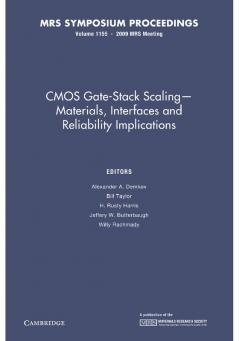
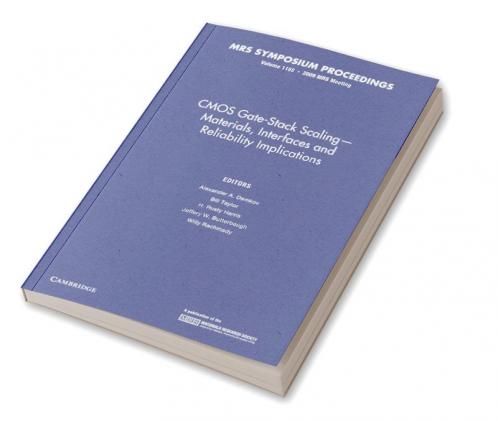
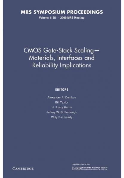
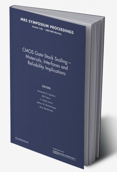
To address the increasing demands of device scaling new materials are being introduced into conventional Si CMOS processing at an unprecedented rate. Presentations collected here focus on understanding from a chemistry and materials perspective the mechanism of interface formation and defects at interfaces for both conventional Si and alternative channel (Ge or III-V) systems. Several papers address reliability concerns for high-k/metal gate (basic physical models charge trapping etc.) while others cover characterization of the thin films and interfaces which comprise the gate stack. Topics include: advanced Si-based gate stacks; and alternate channel materials.
*COD & Shipping Charges may apply on certain items.
Review final details at checkout.
₹3183
Out Of Stock
All inclusive*
Details
ISBN 13
9781107408326
Publication Date
-06-05-2014
Pages
-192
Weight
-268 grams
Dimensions
-152.4x228.6x10.46 mm


