English
Paperback
₹6046
(All inclusive*)
Delivery Options
Please enter pincode to check delivery time.
*COD & Shipping Charges may apply on certain items.
Review final details at checkout.
Looking to place a bulk order? SUBMIT DETAILS
About The Book
Description
Author
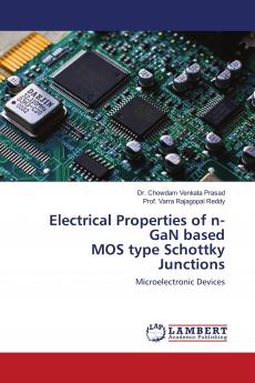
III-nitride semiconductor materials specially gallium nitride (GaN) have attracted significantly in the fabrication of high power high frequency and high temperature devices such as metal/oxide/semiconductor field effect transistors (MOSFETS) heterojunction field effect transistors (HFET’s) and high electron mobility transistors (HEMT’s). However metal/semiconductor (MS) junctions in these devices may suffer from high leakage-current and low break-down voltage which limits the device performance reliability and stability. This could restrain by employing a thin insulator/interlayer between the metal and semiconductor. The formation of high-quality Schottky junctions with low-leakage current and low ideality factor by insertion of a thin insulator/interlayer in the middle of the metal and semiconductor is challenging task. Hence the detailed investigations are prerequisite on the formation of a thin insulator/interlayer in the middle of the metal and semiconductor to achieve high barrier height with low ideality factor and good thermal stability.
Delivery Options
Please enter pincode to check delivery time.
*COD & Shipping Charges may apply on certain items.
Review final details at checkout.
Details
ISBN 13
9786203202168
Publication Date
-13-01-2021
Pages
-152
Weight
-216 grams
Dimensions
-152x229x8.75 mm


