This Book is Out of Stock!
English
Paperback
₹3200
(All inclusive*)
Delivery Options
*COD & Shipping Charges may apply on certain items.
Review final details at checkout.
Looking to place a bulk order? SUBMIT DETAILS
About The Book
Description
Author(s)
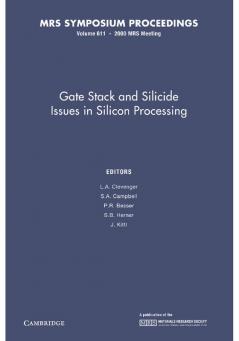
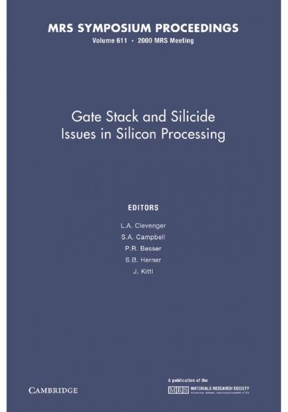
As the feature size of microelectronic devices approaches the deep submicron regime the process development and integration issues related to gate stack and silicide processing are key challenges. Gate leakage is rising due to direct tunneling. Power and reliability concerns are expected to limit the ultimate scaling of SiO2-based insulators to about 1.5nm. Gate insulators must not deleteriously affect the interface quality thermal stability charge trapping or process integration. Metal gate materials and damascene gates are being investigated in conjunction with the application of a high-permittivity gate insulator to provide sufficient device performance at ULSI dimensions. The silicidation process is also coming under pressure. Narrow device widths and decreasing junction depths are making the formation of low-leakage low-resistance silicide straps extremely difficult. Producing shallower junctions via ion implantation is inhibited by transient enhanced diffusion and low beam currents at low implantation energies. Gate stack and contact film effects such as point defect injection extended defect formation and stress on ultrashallow junction formation must be considered.
*COD & Shipping Charges may apply on certain items.
Review final details at checkout.
₹3200
Out Of Stock
All inclusive*
Details
ISBN 13
9781107413160
Publication Date
-06-05-2014
Pages
-252
Weight
-347 grams
Dimensions
-152.4x228.6x13.55 mm


